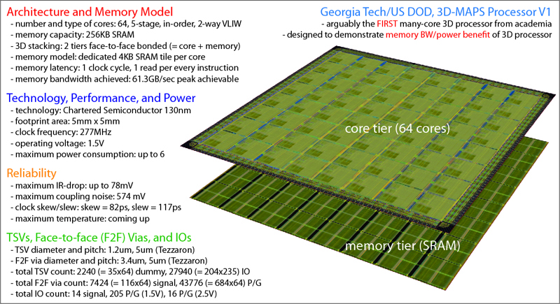
The fabrication of this chip is completed in July 2011 using the 130nm GlobalFoundies device technology and 1.2um TSV diameter Tezzaron technology. The packaging is completed in August 2011 by Amkor. 8 parallel applications are developed to demonstrate the bandwidth and power benefit of 3D MAPS processor. This processor contains 33M transistors, 50K TSVs, and 50K face-to-face connections in 5mm x 5mm footprint and 0.8mm thickness.
The core architecture is developed from scratch by our architecture team to benefit from single-cycle access to SRAM. One of the two instructions we issue in one cycle can be memory read/write, so it is possible to access memory at every clock cycle. Our RTL-to-GDSII tool chain is based on commercial tools from Synopsys, Cadence, and Mentor Graphics. Since these tools can only handle 2D ICs, we have developed plug-ins to handle TSVs and 3D stacking.
Here is our CICC 2010 and 3D-TEST 2010 papers on 3D-MAPS V1.
We are currently working on 3D-MAPS V2 that features 128 cores and 2GB DRAM stacked in 5 dies. Here are the differences:
| 3D-MAPS V1 | 3D-MAPS V2 | |
| # of tiers | 2, one logic and one SRAM | 5, two logic and three DRAM |
| # of cores | 64 | 128 |
| logic footprint | 5mm x 5mm | 10mm x 10mm |
| DRAM footprint | - | 20mm x 12mm |
| device technology | 130nm, Globalfoundries | 130nm, Globalfoundries |
| bonding style | face-to-face | face-to-face & face-to-back |
| TSV technology | Tezzaron, 1.2um diam | Tezzaron, 1.2um diam |
| application | memory BW (GB/s) | power consumption (W) |
| AES encryption | 49.5 | 4.032 |
| edge detection | 15.6 | 3.768 |
| histogram | 30.3 | 3.588 |
| k-means clustering | 40.6 | 4.014 |
| matrix multiply | 13.8 | 3.789 |
| median filter | 63.8 | 4.007 |
| motion estimation | 24.1 | 3.830 |
| string search | 8.9 | 3.876 |
The theoretical maximum memory bandwidth 3D-MAPS V1 can achieve is 70.9GB/s, which is computed by 277MHz x 64 (cores) x 4 Bytes (1 word). One of our applications, median filter, got very close to this theoretical value at the lowest power consumption. As a comparison, here are the maximum achievable bandwidth values of the state-of-the-art processor and memory technology (as of Sep 2011):
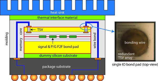
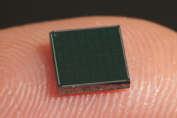
FIGURE 2: The topside of
3D-MAPS V1 is actually the backside of the core die that is thinned down to
12um. With bare eyes, we can only see dummy TSVs and IO cells.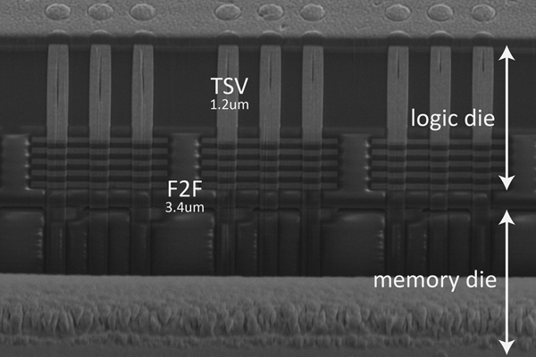
FIGURE 3: SEM image of Tezzaron TSVs and
face-to-face bond pads.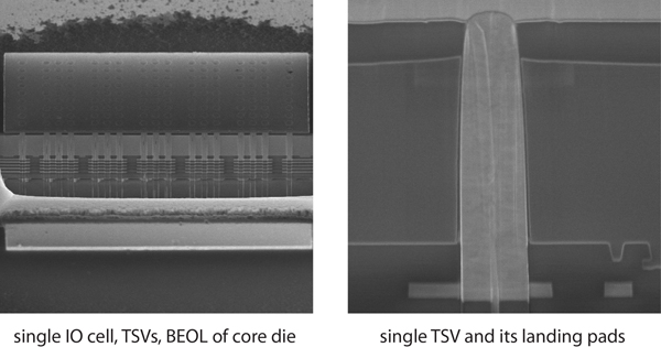
FIGURE 4: More SEM images of TSVs and F2F
pads.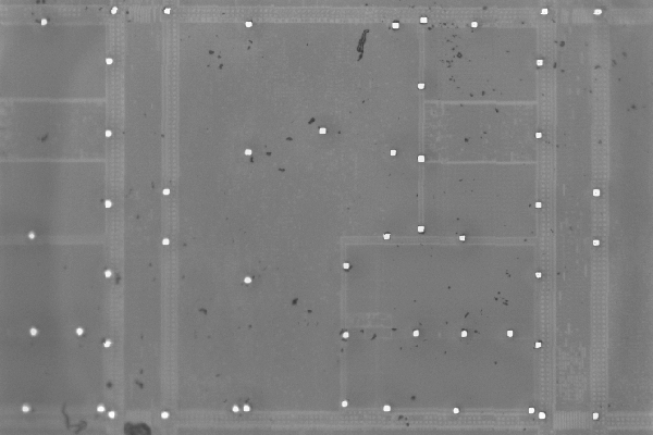
FIGURE 5: The above image is obtained using an
infrared microscope with 6um depth. Since the top surface of 3D-MAPS V1 is the
thinned substrate of top die, we had to use an IR microscope to reveal the
circuitry that is buried under this substrate. The white dots are dummy TSVs we
had to add to satisfy the TSV density rule set by Tezzaron.
FIGURE 6: Some details of single core and
single IO cell.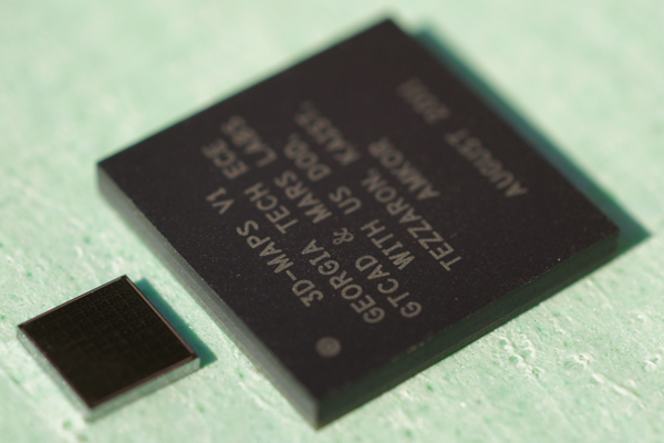
FIGURE 7: Bare die and its package
side-by-side.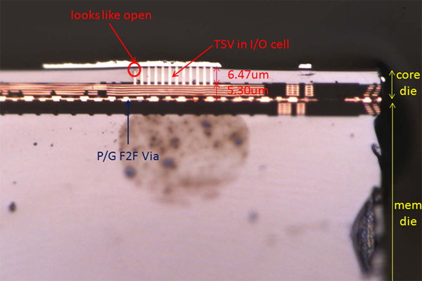
FIGURE 8: The open TSV above, fortunately, does
not cause any problem because all of the TSVs shown are redundant. The top die
(= core die) is thinned down to 12um, and the bottom die (= memory die) height
is 765um, making the total thickness to be roughly 0.8mm.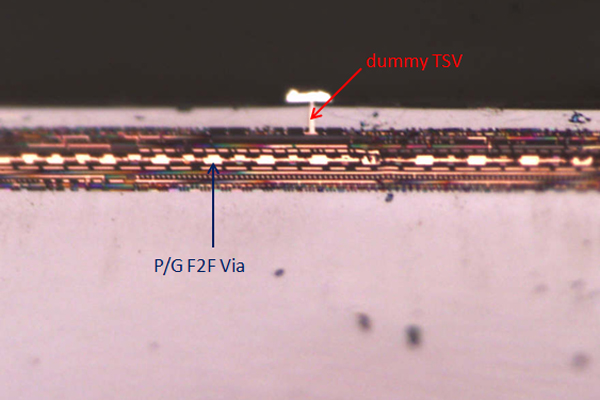
FIGURE 9: A dummy TSV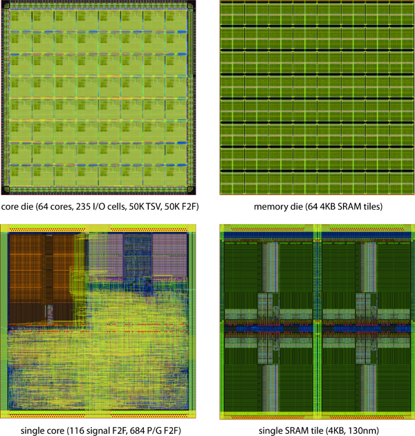
FIGURE 10: Layouts of full-die (core and
memory) and single core/memory tile.